FEI Quanta 3D FEG DualBeam (FIB-SEM)
A dual-beam FIB-SEM combining a field-emission SEM column with a high-current Ga+ focused ion beam. It supports high-vacuum, low-vacuum, and ESEM imaging alongside site-specific milling, cross-sectioning, and gas-assisted deposition for 2D and 3D materials characterization.
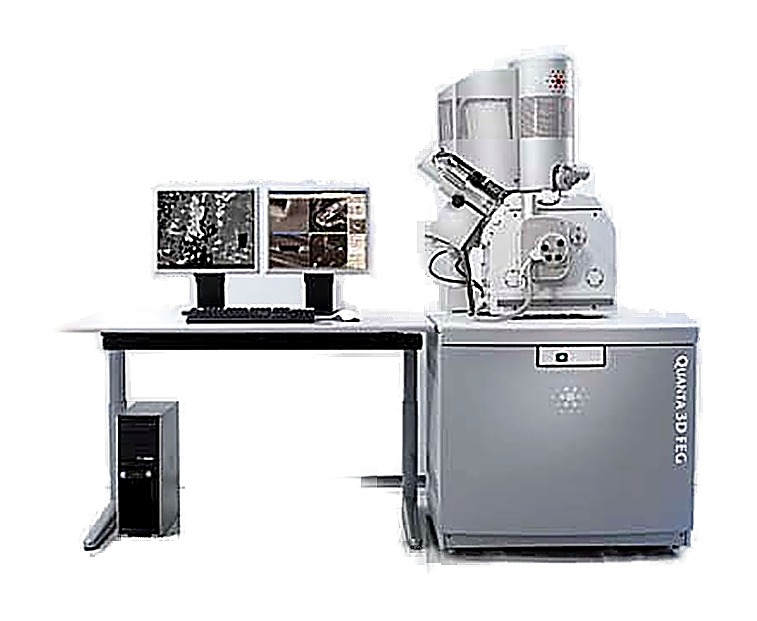
System Capabilities
The Quanta 3D FEG is a versatile high-resolution DualBeam system pairing a field-emission SEM column with a high-current focused ion beam (FIB) for 2D and 3D material characterization. Three electron imaging modes – high-vacuum, low-vacuum, and ESEM – accommodate conductive, non-conductive, and hydrated specimens without additional preparation, including in-situ study of humidity (up to 100% RH) and temperature (up to 1500 °C) effects.
The high-current Ga+ FIB enables fast material removal, automated cross-sectioning recipes, and site-specific milling, while live SEM imaging during milling allows real-time monitoring of the process. A selection of gas chemistries supports material deposition and enhanced or selective etching for both conductive and non-conductive samples.
Operating Modes
High-Vacuum SEM Imaging
Field-emission electron source for high-resolution secondary electron imaging of conductive samples, with backscattered and STEM detection available as optional upgrades.
Low-Vacuum / ESEM Imaging
Charge-free imaging of non-conductive and hydrated specimens up to 4000 Pa and 100% RH.
FIB Milling & Cross-Sectioning
High-current Ga+ ion beam for fast material removal, site-specific cross-sections, and TEM lamella preparation.
Gas-Assisted Deposition & Etch
Multiple gas chemistries for Pt, W, and C deposition plus selective etch to reduce re-deposition during milling.
Technical Specifications
| Electron Source | Field-emission gun, 200 V – 30 kV accelerating voltage |
|---|---|
| Electron Beam Resolution | 1.2 nm at 30 kV (SE, high-vacuum); 2.9 nm at 1 kV (SE) |
| Ion Source | Ga liquid-metal ion source (LMIS), 1000-hour guaranteed lifetime |
| Ion Beam Resolution | 7 nm at 30 kV at beam coincident point (5 nm at optimal working distance) |
| Ion Accelerating Voltage / Probe Current | 2 – 30 kV; 1 pA – 65 nA in 15 steps |
| Chamber Vacuum Modes | High-vacuum < 6×10⁻⁴ Pa; low-vacuum 10–130 Pa; ESEM 10–4000 Pa |
| Motorized Stage | 5-axis eucentric goniometer stage; X/Y 50 mm, Z 25 mm, tilt -15° to +75° |
| Gas Chemistry | Up to 5 gas injectors; Pt, W, Au, and SiO2 deposition; enhanced and insulator etch chemistries |
Comparison: This System vs Conventional Alternative
A high-level comparison to highlight performance and workflow advantages.
| Feature | This System | Conventional Method |
|---|---|---|
| Sample Prep & Imaging | Combined FIB milling and SEM imaging in one chamber | Separate FIB and SEM systems requiring sample transfer |
| Cross-Sectioning | Site-specific, sub-100 nm precision cross-sections | Manual mechanical polishing or sectioning |
| Non-Conductive Samples | Charge-free imaging and milling via low-vacuum/ESEM and charge neutralization | Requires conductive coating |
Common Applications
Accessories
The following accessories expand sample preparation and analysis capabilities for the DualBeam.


Individual accessories may be available for lending, subject to availability.
To inquire about borrowing a specific accessory, please Contact
the Lab Manager.