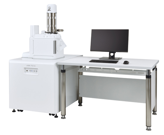
JEOL JSM-IT710HR Field Emission SEM
A Schottky field emission scanning electron microscope for high-resolution imaging and microanalysis. It supports high- and low-vacuum operation with integrated EDS for live spectra and X-ray mapping.
System Capabilities
The JEOL JSM-IT710HR is a compact, multipurpose field emission SEM designed for high-resolution imaging and microanalysis. It delivers high probe current with a small probe size for detailed surface morphology and compositional contrast.
High- and low-vacuum modes accommodate conductive and non-conductive samples, with secondary electron and quadrant backscatter detectors plus live 3D surface reconstruction. Integrated JEOL EDS enables live spectra and X-ray mapping.
Operating Modes
High-Vacuum Imaging
High-resolution SE and BSE imaging for conductive or coated samples.
Low-Vacuum Imaging
Controlled pressure imaging for poorly conducting or outgassing samples.
Live EDS Analysis
Real-time spectra and X-ray maps during imaging.
3D Surface Reconstruction
Live 3D topography using the quadrant BSE detector.
Technical Specifications
| Electron Source | In-lens Schottky field emission gun |
|---|---|
| Maximum Probe Current | >= 300 nA delivered to specimen |
| Vacuum Modes | High vacuum and low vacuum with one-click switching |
| Detectors | SE and quadrant BSE with live 3D function |
| Integrated Analytics | JEOL EDS for live spectra and X-ray maps |
| Automation | Montage, scripting, remote control, and data management |
Comparison: This System vs Conventional Alternative
A high-level comparison to highlight performance and workflow advantages.
| Feature | This System | Conventional Method |
|---|---|---|
| Precision | Higher accuracy and repeatability | Standard tolerance |
| Workflow | Streamlined and automated | Manual or multi-step |
| Throughput | Faster turnaround | Slower cycle time |