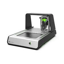
Voltera V-One PCB Printer
A desktop PCB printer for rapid prototyping. The V-One prints conductive ink traces, drills, and supports double-sided and multi-layer PCB workflows for fast iteration.
This equipment is reserved for educational purposes and cannot be independently reserved. For access or more information, please contact the Lab Manager.
System Capabilities
The V-One enables in-house PCB prototyping by printing conductive ink traces and drilling vias. It supports double-sided boards and can be used in multi-layer workflows for rapid design iteration.
The system is designed for quick turnaround of custom PCB designs without external fabrication lead times.
Operating Modes
Trace Printing
Print conductive ink traces directly on PCB substrates.
Drilling
Integrated drilling for vias and through-holes.
Double-Sided Boards
Print both sides for compact circuit layouts.
Multi-Layer Workflows
Support for 4-layer stacks with alignment processes.
Technical Specifications
| Print Area | 128 x 116 x 3 mm |
|---|---|
| Minimum Trace Width | 0.2 mm |
| Minimum Trace Spacing | 0.2 mm |
| Minimum Drill Size | 0.3 mm |
| Minimum Pad Diameter | 0.6 mm |
| PCB Capability | Double-sided and multi-layer workflows |
Comparison: This System vs Conventional Alternative
A high-level comparison to highlight performance and workflow advantages.
| Feature | This System | Conventional Method |
|---|---|---|
| Precision | Higher accuracy and repeatability | Standard tolerance |
| Workflow | Streamlined and automated | Manual or multi-step |
| Throughput | Faster turnaround | Slower cycle time |