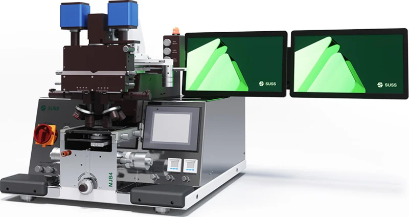
SUSS MJB4 Mask Aligner
A high-precision UV contact aligner designed for research and small-volume production. It aligns a physical photomask with a substrate to transfer micro-scale patterns, optimized for handling fragile materials and III-V semiconductors.
The SUSS MJB4 Mask Aligner is currently offline for lamp replacement and alignment calibration. Service is expected to complete by mid-July 2026. Contact the lab manager for urgent lithography needs or to join the waitlist.
System Capabilities
The SUSS MJB4 is a core photolithography tool in the lab. It enables the transfer of complex geometric patterns from a glass photomask onto a photoresist-coated wafer using UV light.
Its versatile stage design handles irregularly shaped substrates and small pieces, making it ideal for prototyping. The system supports multiple exposure modes, allowing users to balance resolution requirements with substrate safety.
Operating Modes
Soft Contact
Wafer is gently held against the mask. Ideal for fragile substrates to prevent damage.
Hard Contact
Nitrogen pressure pushes wafer firmly against the mask. Standard mode for high resolution (~1 µm).
Vacuum Contact
Removes air between mask and wafer for maximum resolution (~0.5 µm).
Proximity / Gap
Controlled gap (10-50 µm) between mask and wafer. Used for thick resists or 3D topography.
Technical Specifications
| Max Substrate Size | 100 mm (4 inch) Round or Square |
|---|---|
| Mask Size | Standard 2" x 2" up to 5" x 5" |
| Spectrum | Mercury Lamp (g, h, i-line) |
| Resolution (Best Case) | 0.5 µm (Vacuum Contact) |
| Alignment Travel | X/Y: ±5 mm | Theta: ±5° |
| Alignment Accuracy | < 1.0 µm (Topside) |
Comparison: Contact vs. Direct Write
Comparing standard Contact Lithography (SUSS MJB4) against Maskless Direct Write methods.
| Feature | This Tool (Contact Aligner) | Maskless (Direct Write) |
|---|---|---|
| Pattern Source | Physical Photomask (Glass) | Digital CAD File |
| Throughput | High (Full Wafer Exposure) | Low (Serial Beam Writing) |
| Resolution | Diffraction Limited (~0.5 µm) | Beam Spot Limited |
| Cost per Run | Low (After mask purchase) | Free (No mask needed) |
| Flexibility | Low (New mask per design) | High (Instant design change) |