MPI TS200 Manual Probe System
A highly flexible manual probe system designed for analytical characterization of wafers up to 200 mm. It provides a stable, shielded platform for precision I-V/C-V, RF, and mmW measurements on semiconductor devices.
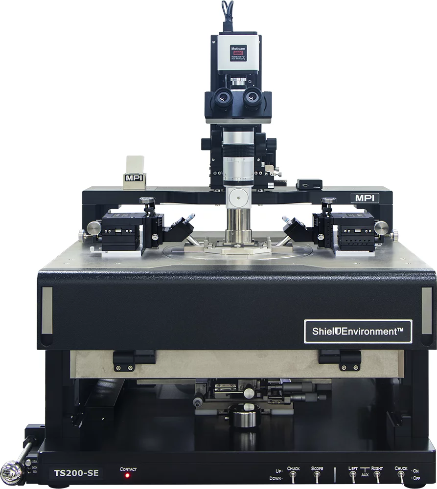
System Capabilities
The TS200 features a modular ShielDEnvironment(TM) for EMI-shielded and light-tight measurements, crucial for low-noise electrical characterization. It supports substrates ranging from small fragments up to 8-inch wafers.
Equipped with independent X-Y-Z and theta controls, the stage ensures accurate alignment for contacting small features. The platen supports a wide variety of micro-positioners (magnetic or vacuum bases) for versatile testing setups.
Operating Modes
DC Probing
Standard I-V and C-V characterization requiring low-noise cables and a shielded environment for pA-level accuracy.
RF & mmW Probing
High-frequency S-parameter testing for filters, antennas, and high-speed circuits using specialized RF probes.
Thermal Testing
Characterizing electrical properties under thermal stress (Ambient to 300°C standard, expandable to -60°C).
Failure Analysis
Signal tracing on ICs to identify local defects or shorts, best performed with high-magnification optics.
Technical Specifications
| Chuck Size | 200 mm (8 inches) |
|---|---|
| X-Y Travel Range | 205 mm x 205 mm |
| Chuck Z-Stroke | 10 mm (for safe loading) |
| Chuck Planarity | < 10 µm across 200 mm |
| Microscope Travel | 50 mm x 50 mm (X-Y) with Z-lift |
| Platen Material | Steel or Aluminum (High Rigidity) |
Comparison: On-Wafer vs. Packaged Testing
Comparing manual on-wafer probing (TS200) against traditional packaged device testing.
| Feature | TS200 (On-Wafer Probe) | Packaged Testing |
|---|---|---|
| Device State | Bare Die / Wafer | Encapsulated / Bonded |
| Feedback Speed | Immediate (Fab Line) | Delayed (After Packaging) |
| Cost per Test | Low (No Package needed) | Higher (Requires Packaging) |
| Interface | Direct Micro-Probe | Sockets / PCB Solder |
| Signal Integrity | High (Minimal Parasitics) | Variable (Package Parasitics) |