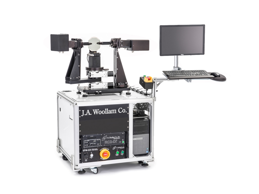
J.A. Woollam RC2 Ellipsometer
High-speed dual-rotating compensator spectroscopic ellipsometer for non-contact thin film characterization. Provides full Mueller-matrix data, mapping, and precision thickness and optical constants.
System Capabilities
The RC2 uses a dual-rotating compensator design to capture full Mueller-matrix data, enabling characterization of complex, anisotropic, or depolarizing samples.
High-speed acquisition allows more than 1000 wavelengths per measurement and supports automated mapping for uniformity checks across wafers or large substrates.
Operating Modes
Spectroscopic Ellipsometry
Thin film thickness and optical constant measurements (n, k).
Mueller-Matrix
Full 16-element Mueller matrix for complex materials.
Mapping
Spatial uniformity of thickness and optical constants.
In-Situ Monitoring
Real-time growth or etch rate monitoring (with integration).
Technical Specifications
| Spectral Range | UV-Vis-NIR (210 nm to 1690 nm or 2500 nm) |
|---|---|
| Detectors | CCD (UV-Vis) and InGaAs (NIR) |
| Angle of Incidence | Automated or manual, typically 45 to 90 deg |
| Data Acquisition | ~0.1 to 3 seconds per measurement point |
| Wavelength Count | >1000 channels per measurement |
| Sample Size | Standard configurations up to 200 mm or 300 mm wafers |
| Sample Surface | Reflective or semi-reflective surfaces preferred |
Comparison: Ellipsometry vs. Stylus Profilometry
Comparing optical ellipsometry to traditional contact profilometry.
| Feature | This System (Ellipsometry) | Traditional Method (Stylus Profilometer) |
|---|---|---|
| Measurement Method | Non-contact optical polarization analysis | Contact stylus traces surface topography |
| Data Output | Thickness and optical constants (n, k) | Step height and surface profile |
| Sample Impact | Non-destructive, no surface contact | Physical stylus contact with surface |
| Mapping | Automated multi-point mapping | Line scans with limited area coverage |
| Best Use | Thin film characterization and optical properties | Step height and roughness verification |